accomplish using most of the other
nanofabrication techniques. New advances in chemical vapor deposition such as ‘initiated chemical vapor deposition’ (i-CVD) provide unprecedented opportunities of depositing polymers without reduction in the molecular weights
Allows high-precision assembling of Many issues need to explore, such as Very early stage. Ultimate success nanoscale components into novel unit and integration processes, depends on the willingness of the programmable arrangements with compatibility with CMOS fabrication, semiconductor industry in terms of much smaller dimensions (less than line edge roughness, throughput and need, infrastructural capital investment, 10 nm in half-pitch) cost yield and manufacturing cost
DNA-
scaffolding
materials including metal, ceramics,
semiconductors, insulators and polymers, high purity nanofilms, a scalable process, possibility to deposit porous nanofilms
General remarks
Demerits
Merits
Bottom–up
method
Table 1 (continued)
-
Characterization of NPs
915
-
Morphological characterizations 915
-
Structural characterizations 916
-
Particle size and surface area characterization 918
-
Optical characterizations 919
-
Characterization of NPs
Different characterization techniques have been
practiced for the analysis of various physicochemical properties of NPs. These
include techniques such as X-ray diffraction
(XRD), X-ray photoelectron spectroscopy (XPS), infrared (IR), SEM, TEM,
Brunauer–Emmett–Teller (BET), and particle size
analysis.
-
Morphological characterizations
The morphological features of NPs always attain
great interest since
morphology always influences most of the properties of
the NPs. There are different characterization techniques for
Scheme 3
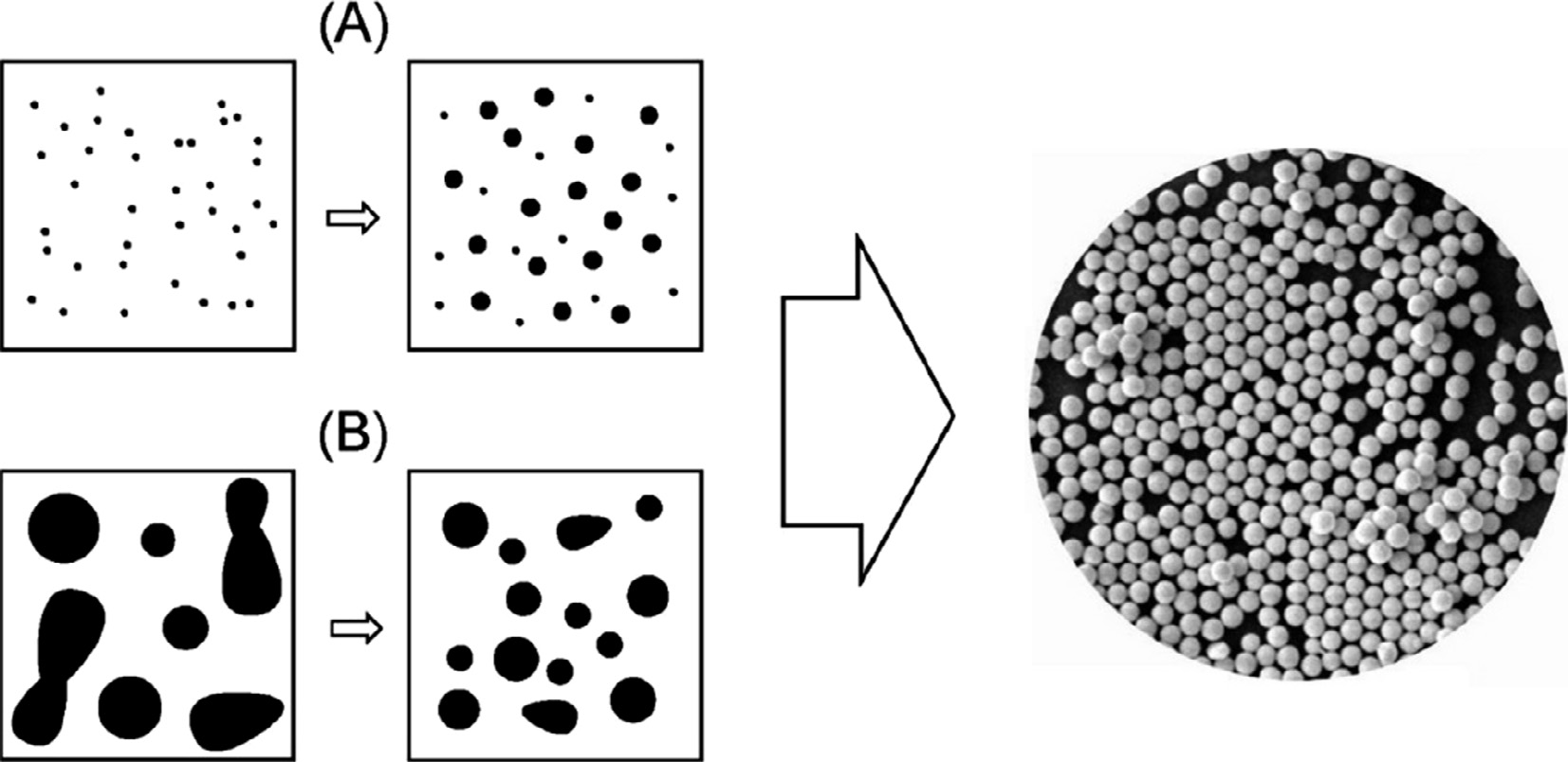
(A) Bottom-up approach: A molecular precursor is disintegrated to simpler metal atoms that grow into colloids. (B) Top- down approach: Large drops of a metal broken into smaller drops (Wang and Xia, 2004).
morphological studies, but microscopic techniques such as polarized
optical microscopy (POM), SEM and TEM are the
most important of these.
SEM
technique is based on electron scanning principle,
and it provides all available information about the
NPs at nanos- cale level. Wide literature is
available, where people used this technique
to study not only the morphology of their nanoma-
terials, but
also the dispersion
of NPs in the bulk or
matrix. The dispersion of SWNTs in the polymer
matrix poly(buty- lene)
terephthalate (PBT) and nylon-6 revealed through this
technique (Saeed and
Khan, 2016, 2014). The same
group also provides POM study of their materials,
which showed star-like spherulites
of the formed materials, whose size was decreased
with the incremental filling of SWNTs. The morphological fea- tures of ZnO modified metal organic frameworks (MOFs) were studied
through SEM technique, which indicates the ZnO NPs
dispersion and morphologies
of MOFs at different reaction conditions (Fig. 7) (Mirzadeh and Akhbari, 2016).
Similarly, TEM is based on electron transmittance princi- ple, so it
can provide information of the bulk material from
very low to higher magnification. The different
morphologies of gold NPs are studied via this
technique. Fig. 8 provides some TEM
micrographs showing various morphologies of
gold NPs, prepared via different methods
(Khlebtsov and Dykman,
2011, 2010a, 2010b). TEM also
provides essential information
about two or more layer materials, such as the
quadrupolar hollow shell structure of
Co3O4 NPs
observed through TEM. These NPs founded to be exceptionally active as anode in Li-ion batteries
(Fig. 9). Porous multishell struc- ture
induces shorter Li+ diffusion
path length with adequate annulled
space to buffer the volume expansion, good cycling performance, greater rate capacity, and specific
capacity as well (Wang et al., 2013).
-
Structural characterizations
The structural characteristics are of the primary
importance to study the composition and nature of
bonding materials. It pro- vides diverse information about the bulk properties of the sub-
ject material. XRD, energy dispersive X-ray
(EDX), XPS, IR, Raman, BET,
and Zieta size analyzer are the common tech-
niques used to study structural properties of NPs.
XRD is one of the most important characterization
tech- niques to reveal the structural properties of NPs. It gives enough information about the
crystallinity and phase of NPs. It also provides rough idea about the
particle size through Debye Scherer formula
(Khan et al., 2017b,
2017c; Ullah et al.,
2017). This
technique worked well in both single and
multiphase NPs identification (Emery et
al., 2016).
Never- theless, in the case of smaller NPs having
size less than hun- dreds of
atoms, the acquisition and correct measurement of
structural and other parameters may be difficult.
Moreover, NPs having more amorphous characteristics
with varied inter atomic
lengths can influence the XRD diffractogram. In that
case, proper comparison of the diffractograms of
bimetallic NPs with those of the corresponding
monometallic NPs and their
physical mixtures is required to obtain accurate
informa- tion. Comparison of computer simulated
structural model of bimetallic NPs with observed XRD spectra is the best way to get good
contrast (Ingham, 2015). EDX,
which is normally fixed with
field emission scanning electron miscopy (FE-SEM)
or TEM device is widely used to know about the
elemental composition with a rough idea of % wt. The
electron beam focused over a single NP by SEM or TEM
through the pro- gram functions, to acquire the insight information from the NP under
observation. NP comprises of constituent elements
and each of them emits characteristics energy
X-rays by elec- tron beam irradiation. The intensity of specific X-ray is directly proportional to the concentration of the explicit
element in the particle.
This technique is widely used by researchers to give
support to SEM and
other techniques for the confirmation of their
elements in prepared materials (Avasare et
al., 2015; Iqbal et al., 2016). The EDX
technique used to determine the
elemental composition of ultra-sonochemically
synthesized pseudo-flower shaped
BiVO4 NPs
(Khan et al.,
2017b).
Simi- larly, by utilizing similar technique the
elemental confirmation and
graphene impregnation of In2O3/graphene
heterostructure NPs was carried out, which showed C, In and O as contribut-
Table 1 Top-down and bottom-up synthetic techniques with merits, demerits and general remarks (Biswas et al., 2012).
Top–down method
Merits Demerits General
remarks
Optical lithography
E-beam lithography
Soft and nanoimprint
lithography
Block co- polymer lithography
Scanning probe lithography
Long-standing, established micro/nanofabrication tool
especially for chip production, sufficient level of resolution at high throughputs
Popular in
research environments, an extremely accurate method and effective nanofabrication tool for <20 nm nanostructure fabrication with
desired shape
Pattern transfer based simple, effective nanofabrication tool for fabricating ultra-small features (<10 nm)
A high-throughput, low-cost method, suitable for large-scale densely packed nanostructures, diverse shapes of nanostructures, including spheres, cylinders, lamellae possible to fabricate including parallel assembly
High resolution chemical, molecular and mechanical nanopatterning capabilities, accurately controlled
nanopatterns in resists for transfer to silicon,
ability to manipulate big molecules
and individual atoms
Tradeoff between resist process sensitivity and
 ЖИ көмекші


 Жүктеу

 Бұл курс Қазақстан Республикасы Оқу-ағарту министрлігімен келісілген